| EEL
6323 |
 |
|
|
The following is an example of a simple CMOS inverter using the TSMC 0.18-micron technology, showing all the steps one would perform for a typical design. Please be patient while all the images load...
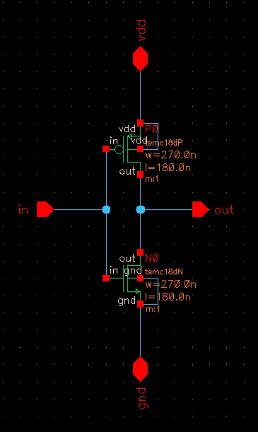
Schematic
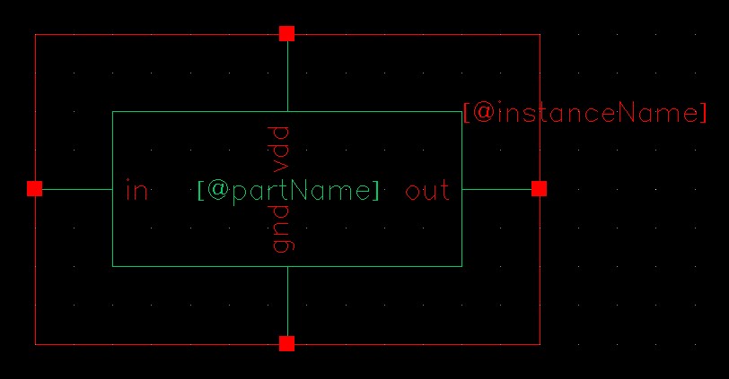
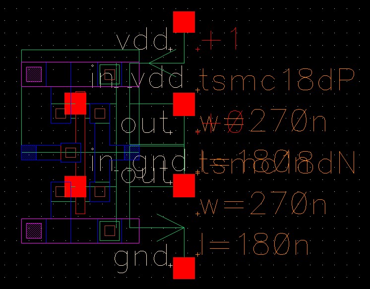
Symbol
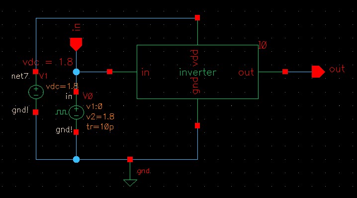
Test Schematic
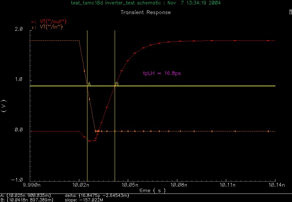
Schematic Simulation
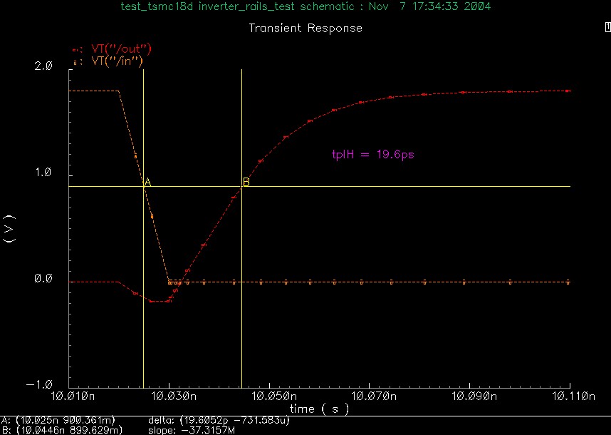
| The following shows the results of the schematic-level simulation. This form of simulation is useful to test functional correctness of the design and to obtain preliminary timing data. However, it is important to keep in mind that it does not take into account any effects contributed by the physical layout process. |
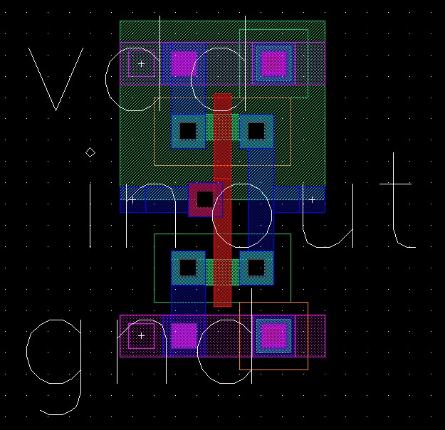
Layout
Extraction
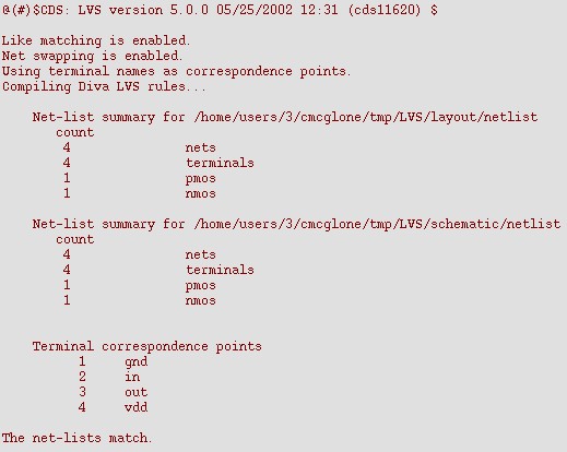
LVS
| The most important line in the LVS output file is shown here at the bottom: "The net-lists match". This guarantees the schematic and layout contain precisely the same devices connected precisely the same way. |
Layout for Parasitics
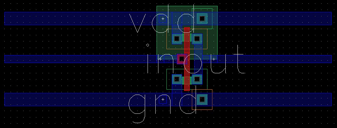
| By itself, the layout of the 0.18-micron minimum-sized inverter contains only negligible parasitics. However, in a real design this inverter would be part of a larger layout, driven by some preceeding logic stage and, in turn, driving one or more gates in a subsequent stage, all connected by interconnect. To demonstrate the influence of interconnect parasitics, the original layout was modified as shown below, extending the power rails and input/output lines as might realistically be done during the signal routing phase of design. |
Parasitics Extraction
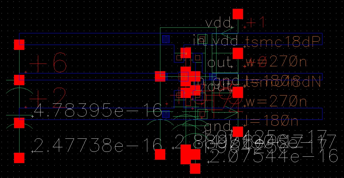
| Although perhaps difficult to read, the layout extracted with parasitics shown below has small capacitors associated with the metal power rails. These are on the order of 10^-16 F (a few tenths of a femto-Farad). |
Layout Simulation
| Shown below are the simulation results for the extracted layout containing the interconnect parasitics. Compared to the simulation of the schematic (neglecting any parasitics) shown above, the low-to-high propagation delay has increased about 17%. |