Getting Started
 | Running
Cadence
 | Cadence is a commercial UNIX application licensed
to UF for academic use. It
can only execute on a machine running the UNIX operating system and is
not available for installation on personal machines. |
| With
that said, you can still use Cadence on a PC via a remote connection (toons.ecel.ufl.edu)
in conjunction with X server software (Cygwin).
 | All
PCs in the 2nd floor NEB computer lab already have Cygwin
installed. Directions
for usage can be found here. |
| Cygwin
is also available as freeware for installation at home.
Their website is http://www.cygwin.com/. |
|
| UF
engineering
students have three options for running cadence:
| Natively
on the Sun workstations in the 2nd floor NEB computer lab
(easiest, most direct method) |
| Remotely
on the PC workstations in the 2nd floor NEB computer lab
using Cygwin (more difficult, slightly slower method) |
| Remotely
on a home workstation (most flexible, but somewhat slower method)
| Only
consider this option if you have broadband as Cadence requires a
lot of display information to be passed back and forth. |
|
|
| Click
here for Step-by-Step Remote Setup
instructions. |
|
| Using
UNIX
| Since
Cadence is a UNIX application, you’ll want some minimal proficiency
using the operating system. The
basic interface to UNIX is the shell, which is a command-line
interpreter similar to DOS. You’ll
use the shell to organize your files, perform basic file maintenance,
and launch the Cadence application. |
| If
you’ve never used UNIX, several online tutorials exist to get you up
to speed. Here are a
couple:
|
|
| Setting
Up Cadence
| You
should be able to run Cadence without any special setup process. However, if you
want to customize the environment and/or the way Cadence starts, you can
copy the following files to your home directory and change them
accordingly (consult the Cadence online documentation for more info):
| /usr/local/cadence/local/.cdsenv -
environment settings |
| /usr/local/cadence/local/.cdsinit -
initialization settings |
| /usr/local/cadence/local/cdssetup/cds.lib -
library index |
|
| The cds.lib file becomes important
if you want access to additional technologies that are not part of the
default Cadence installation. A technology is a collection of device parameters, models, and
fabrication data that is available to Cadence for use in designs. Using
the default library list is fine, but if you need access to additional
technologies, you will need to manually add them to the cds.lib file. |
| The following environment variables should
already be set by your default shell profile, but if you encounter
trouble running Cadence, you can double-check to make sure they are set
correctly.
| CDS_INST_DIR=/usr/local/cadence/ic50
| To verify, enter echo $CDS_INST_DIR |
| To set, enter export CDS_INST_DIR=/usr/local/cadence/ic50 |
|
| PATH should include /usr/local/bin
| To verify, enter echo $PATH |
| To set, enter export PATH=$PATH:/usr/local/bin |
|
|
|
| Starting Cadence
| To start Cadence, type icfb from a shell
window. If you are starting a new project, you may want to create
a fresh directory and switch into it first; this will keep your work for
different projects separate. If you are continuing work on an
existing project, change to the appropriate directory before starting.
|
| When Cadence starts up, two windows should appear (if
they don't and you're
running on a PC, it most likely means there's something wrong with your
remote
setup):
| icfb Log - all output from the various
Cadence commands go to this window; when in doubt as to whether or
not something worked or to obtain more information on why something
didn't work, check the information in this window. Also, there
is a command prompt available at the bottom of this window by which
you can directly enter commands if necessary (not used very often). |
| Library Manager - this window shows
the contents of your current project. You should see three
sub-panes labeled Library, Cell, and View, corresponding to the
different levels of project hierarchy used by Cadence.
| Library - this is the top level of
hierarchy; a library contains one or more cells. An entire
project may be contained in a single library or could be divided
across several. One useful method is to place all
production (i.e. finished) cells in one library and all testing
cells in another. Also, the design technologies used by
Cadence are organized as individual libraries (i.e. a particular
technology has a single library that defines it). |
| Cell - this is the smallest design
unit of self-contained functionality that, collectively, defines
the contents of your project. Common fundamental cells
might be an inverter, two-input NAND gate, etc. Cells can
themselves be defined in terms of other existing cells (another
form of hierarchy supported by Cadence; more on this
later). A cell has one or more views that define it. |
| View - this is where you define
the behavior of your cell. Many different types are
possible, only some of which we will be interested in.
They are listed below:
| Schematic - transistor-level
(usually) diagram of the cell; designed using the Composer
tool |
| Symbol - single block that can
be used by other cells; the top-level interface signals of
the cell are present as pins in the symbol; designed using
the Composer tool |
| Layout - physical-level
diagram of the cell; designed using the Virtuoso tool |
| Extracted - physical-level
diagram of the cell containing explicit indication of all
well-formed transistors and all layout-related parasitics;
automatically generated by the extraction process |
|
|
|
|
Starting a Project
| Starting a New Project
| To start a new project, first create a
library. Click on File->New->Library within the
Library Manager window. |
|
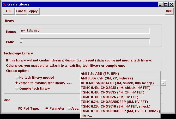
Once you have selected and entered
a name for the library, click on the Attach to existing tech
library button. In the drop down menu list to the right,
several technologies should appear as shown below. These
technologies were obtained from the cds.lib file (either
the default or one you modified).
|
|
NOTE: Selecting the right
technology to use for your design is crucial!!
|
Not all technologies have full
Cadence support for all tools (schematic, simulation, layout). |
|
Changing tech libraries after
you have started is possible, but often leads to unexpected behavior
-- it is much better to choose the right one from the start. |
|
A suitable technology for basic
CMOS design which has been tested and verified to work is Agilent's HP
0.60u AMOS14TB. This
technology is a 3.3V CMOS n-well process containing 3 metal layers
and 1 poly layer. Additional information on the technology is
available from MOSIS here. |
|
Feel free to experiment with
other technologies. However, it is always a good idea to
perform a basic sanity test (e.g. an inverter) with the technology
before investing a lot of design time. |
|
|
Once you are happy with your
selections, click OK to create the library. |
|
|
Creating a New Cell View
|
To create a new cell view, verify
your desired library is highlighted in the left pane and click on File->New->Cell
View within the Library Manager window. |
|
If the cell view is for an existing
cell, verify its name is listed in the Cell Name box of the
Create New File window that appears (or enter it if it is
not). If the view is for a new cell, enter the desired cell name
in the box. |
|
Then select the desired tool from
the drop-down list: Composer-Schematic for a schematic, Virtuoso
for a layout; these are the two primary tools you will be using in this
course. |
|
Once the tool is selected, the View
Name box contents will adjust automatically to match. There
is no need to change the contents of this field unless you intend to
have multiple view of the same type for a single cell (unlikely except
in unusual circumstances). |
|
Click OK to create the
cell view. The corresponding tool will automatically open to edit
the new view. |
|
|
Other Cell Operations
|
To open an existing cell view,
simply double-click on its view name within the Library Manager. |
|
Cells can be copied, moved, and
deleted within a library and between libraries as needed.
Right-click on the desired cell for these additional options, or select
them from the Edit menu of the Library Manager. |
|
The Design Process
|
Process Design Flow
|
Basic digital CMOS design can be
done in the following steps with Cadence:
-
Design a transistor-level
schematic of your cell using Composer; make use of global supply
nets such as VDD and GND, but do not include any stimulus in your
circuit (i.e. voltage sources, etc.).
-
Make a symbol of your cell via
Composer.
-
Create a new testing cell with
a schematic view that instantiates one instance of the symbol you
made in step 2 along with any external sources required for
stimulus. Don't forget to define VDD with a DC source.
-
Simulate the testing cell using
Spectre/SpectreS (depending on technology) to verify base
functionality. This stage can also be used to obtain proper
relative transistor sizings for each of the gates in your design.
-
Layout your cell from step 1
using Virtuoso, running the Design Rule Check (DRC) tool frequently
to verify your layout complies to the restrictions mandated by your
technology.
-
Run the Extract tool on the
finished layout to create an extracted cell view.
-
Open the extracted cell view
and run the Layout Versus Schematic (LVS) tool to guarantee your
views are functionally identical. Revise your layout as needed
until the netlists match.
-
(Optional) For our
purposes, we can usually stop here for most designs. At this
point we have designed, simulated, laid out, and verified our
cell. However, we have not yet simulated our circuit with the
parasitic effects of the layout included in the analysis. A
poor layout can detrimentally effect the dynamic performance of our
circuit, and in extreme cases, cause our design to fail. A
final step is to re-extract the layout with parasitic effects
included and re-simulate the testing cell using the extracted data
instead of the schematic data.
-
Repeat steps 1-8 for all
additional cells in the design. Take advantage of hierarchy to
minimize your work and maximize your efficiency.
|
|
|
Using Schematic Composer
|
Designing a schematic using the
Composer tool consists of the following steps:
-
Enter instances of all
components required by the cell (transistors, passive devices, and
other user cells).
-
Wire components together.
-
Add I/O pins.
-
Check and save.
|
|
To enter a component instance,
click on Add->Instance. Most common options in Composer have a
shortcut button on the left-hand side and a shortcut key in addition to
being listed under one of the menus. |
|
This will bring up the Component
Browser window. First select the library from which you would like
to select a component. Occasionally, the technology library you
are designing with will have custom parts available in Composer that you
can use. However, most often they will not, and you will instead
want to use the components in the NCSU_Analog_Parts library. When
you select a component from the analog parts library, Cadence will
automatically associate the appropriate model from your technology
library with the part if it is available. Below is a list of the
NCSU_Analog_Parts components you will most often deal with:
|
N_Transistors->nmos4 -
4-terminal standard NMOS transistor; in general, you will want to
use the 4-port version so that you can explicitly include your
substrate connection; this will be important when running the LVS
tool.
|
|
P_Transistors->pmos4 - PMOS
counterpart of the nmos4 part
|
|
R_L_C->res - resistor
|
|
R_L_C->cap - capacitor
|
|
R_L_C->ind - inductor
|
|
Supply_Nets->vdd - global
VDD terminal
|
|
Supply_Nets->gnd - global
GND terminal
|
|
Voltage_Sources->vdc - DC
voltage source
|
|
Voltage_Sources->vpulse -
pulse voltage source (i.e. square-wave)
|
|
Voltage_Sources->vpwl -
piece-wise linear voltage source, useful for driving digital
circuits with arbitrary bit vectors (e.g. 100111011001...)
|
|
Voltage_Sources->vsin -
sinusoidal voltage source
|
|
|
Once you've selected the part, you
can modify its properties in the Add Instance window before clicking on the
schematic to place the part. In particular, you can set the W/L
ratios of your NMOS and PMOS transistors if necessary. |
|
When you're done placing all your
parts, enter Esc to exit the add instance mode. In general, hit
Esc anytime you want to stop what you're currently doing and return to
normal mode. |
|
To wire your parts together, click
Add->Wire (narrow) from the menu bar, or click on the wire tool button on
the side (or use the shortcut key w). Click on the terminals of your
components to route wire between them. Press Esc when you are
finished. |
|
To add your I/O pins, click Add->Pin
and enter one or more names in the Pin Names box separated by
spaces. One by one, select the appropriate directivity for the pin
from the drop-down list and then click on the schematic to place the
pin. Hit Esc when you are done. |
|
Click Design->Check and
Save to save your work. If there are any errors or
warnings, check the Log window for more information. |
|
|
Creating a Symbol
|
coming soon... |
|
|
Simulating Your Schematic
|
coming soon... |
|
|
Using Virtuoso
|
coming soon... |
|
|
Extracting Your Layout
|
coming soon... |
|
|
Running LVS
|
coming soon... |
|
|
Simulating Your Layout
|
coming soon... |
|
| Submitting Your Layout
|
When you are completely finished
with your layout, you can export your design into a single file for
easier electronic submission (e.g. for fabrication, or, in our case, for
grading). There are several standard file formats used in the
industry; we will be using the GDS II stream format, which is a binary
format. |
|
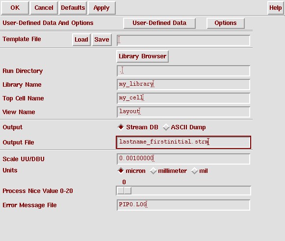
To generate the output file, select
File->Export->Stream from the Log window. In the window that
appears, click on Library Browser and select the library and cell
corresponding to the design you wish to export. Then select a name
for the output file, preferably your last name, followed by an
underscore, and then your first initial, for identification
purposes. When you are done, click OK. A sample
dialog window is shown below. |
|
Check the Log window for the results of the export
process. There may very well be one or more warnings generated which
should be able to be ignored safely. Just double-check that no errors
occurred and that the output file was created and is of reasonable size (on
the order of a few kilobytes for small designs). If you want, you can
re-import the stream file you just created to verify the layout information
is intact. |
|
The stream file can now be sent
electronically as an e-mail attachment. |
|
Additional References
| Excellent 3-part tutorial of an inverter from
Michigan State University:
|
|