| EEL
6323 |
 |
|
|
Questions
- Members of my team want to be able to work individually on different portions of the design and then combine the results. How can we share our work?
- What type of information should I be sure to include in my final SRAM Data Sheet?
- What are the layout design rules I should use for my technology?
- How do I construct a pad frame using the TSMC 0.24u CMOS025/DEEP technology?
- What information should I include in my final project report?
Answers
- Members of my team want to be able to work individually on different portions of the design and then combine the results. How can we share our work?
Fortunately, Cadence helps make this a little easier by using an intuitive hierarchy of directories to store information related to a single design. A Cadence library corresponds to a single directory in the Unix hierarchy. Each of the cells present in the library correspond to a single directory under the library directory. The cell directory contains further subdirectories for each of the cell views defined for that cell. So sharing cells developed by different group members amounts to sharing directories. There are several ways to do this; here are a couple:
- Have each team member e-mail all the members in the team with their personal cell directories as an e-mail attachment. That way, each team member will have all the latest cells contained in the project. You can use the Unix
tarcommand to consolidate an entire directory (along with its contents) into a single file:
- In your Unix window, change into the library directory you're using for the project.
- Run the command:
where you replace
tar -cvf my_tar_file.tar cell_directory
my_tar_file.tarwith whatever you want to call the new file andcell_directorywith the name of the cell you want to share. This will consolidate all the data associated with your cell into a single file for easier e-mailing. You can repeat this for each of the cells you want to share.- Create an e-mail, attach the new file, and send it to your team members.
- When your team members receive it, they can download it to their Unix account, change directories into their project library directory, and run the command:
where
tar -xvf my_tar_file.tar
my_tar_file.taris the name of the attached file. This will extract the contents of the file and create any necessary directories so that the cell data is ready to use.- If you plan to share cells frequently, e-mailing can become a hassle. Another option is to copy cell directories directly from one user account to another. Here's one possible setup:
- Appoint one member of your team as the Team Librarian (preferably whomever is the most Unix-savvy person on your team). This person will use their account as the central sharing location to which all other team members can copy their updates and from which team members can get fresh copies of the latest version of the project.
- The Team Librarian must first make their home directory world readable and executable (searchable) by executing the following from his/her home directory:
chmod 755 .
Don't forget the period; it indicates the current directory (home).- The Team Librarian must then create a directory in their home Unix directory (
mkdircommand) and change the permissions to globally readable/writeable. This can be done with the command:
chmod 777 directory_name
wheredirectory_nameis the new directory.- When a member has completed work on a cell and is ready to share it with a team, s/he executes the following command:
cp -r cell_directory team_librarian_directory
whereteam_librarian_directoryis the name of the global directory that your Team Librarian created in their home directory. Use the tilde (~) to access the home directory of your Team Librarian (example:~cmcglone/publicis the path to a directory in the T.A.'s home directory).- The team member must then execute the following command to change permissions on the newly created directory (failure to execute this step will prevent the Team Librarian from being able to remove the new files at a later time):
chmod 777 new_cell_directory
wherenew_cell_directoryis the path to the newly created cell directory under the Team Librarian's global directory.- Depending on the way the Team Librarian chooses to organize the global directory, the cell updates may be copied directly to the appropriate place in the project hierarchy so that the project directory is always up-to-date. Or, to prevent possible overwrites, breakages, etc., it might be better to use a buffer area as a go-between. Once the Team Librarian has verified any newly updated cells work correctly in the design, s/he can copy them to the global project directory so that other team members can make a fresh copy to get the latest version of the project to work with.
- To get the latest copy, each team member can run the following:
cp -r global_project_directory .
whereglobal_project_directoryis the location within the Team Librarian area which contains the latest version.- WARNING: It is important to realize that the Team Librarian area is world-writeable. Thus, in theory at least, it is subject to attack and/or abuse by other users on the system who are so inclined. Use this method at your own risk and be sure to make frequent backups (in a non-globally-writeable location) of your work. You are solely responsible for any repercussions resulting from use and/or abuse of your Unix account.
Last but not least, if you're going to share cells between different user accounts, be sure to agree on conventions for the design BEFORE you start working. If not, you run the risk of trying to combine cells that are not compatible with each other, and paying for it with lost time.
- What type of
information should I be sure to include in my final SRAM Data Sheet?
Certainly browse around online at some existing commercial data sheets to get an idea as to some of the standard types of information. Here's a list of a some items you'll want to consider including, where applicable for your design:
- Feature Summary
- General Description
- Functional Block Diagram
- Pin Diagram with Pin Descriptions
- Detailed Functional Description
- Truth Table
- Recommended Operating Conditions (temperature, voltage, etc.)
- Absolute Maximum Ratings (supply, frequency, etc.)
- Electrical Characteristics (input capacitance, driving capability, active power, standby power, etc.)
- Timing Waveforms (showing signal transitions for each operation along with setup, hold, and delay times)
- What are the layout design rules I
should use for my technology?
Information regarding design rules for each of the fabrication technologies supported by MOSIS is available on their website here. MOSIS supports 3 separate flavors of design rules; depending on your selection of fabrication technology and your choice for lambda (half the minimum feature size), you will want to use one of the 3 design rule sets:
-
SCMOS - Scalable CMOS design rules, originally developed for processes with feature sizes greater than 1.0 µm.
-
SCMOS_SUBM - Sub-Micron Scalable CMOS design rules, enhanced from SCMOS to better fit processes with feature sizes below 1.0 µm.
-
SCMOS_DEEP - Deep-sub-micron Scalable CMOS design rules, enhanced from SCMOS_SUBM to better fit processes with feature sizes at and below 0.25 µm.
Links to design rules for some tested technologies are available under the Technology Setup page here. After clicking the appropriate link, you will be brought to a page containing the Layer Map specific to the chosen technology. The Layer Map contains all the process layers that are available to that fabrication process. Clicking on any of the layer links will bring up a page containing all the design rules associated with that layer. Be sure to use the correct lambda column (SCMOS, SUBM, or DEEP) depending on your chosen technology.
-
- How do I construct a pad frame using
the TSMC 0.24u
CMOS025/DEEP technology?
The MOSIS Pad Library webpage is located here. Consult the information provided for TSMC 0.25. The pad library is available for download in both CIF and GDS formats. Documentation on the pad library is also available from the MOSIS website in PDF format. To get access to the pad cell library in Cadence, you must select one of the following options:
- Download the pad library from the MOSIS website
(I suggest GDS format) and use Cadence's import function (
File->Import->Streamfrom ICFB window) to load the pad library. You will need to explicitly specify the ASCII technology file corresponding to the CMOS025/DEEP process. If you don't know what that is, you may reference it directly from~cmcglone/public/tsmc25d.tfor download it directly here. After importing, you will have to attach your new pad library to the CMOS025/DEEP technology manually (Edit->Attach tech library...from Library Manager). (This is the more difficult option.) - Reference the pad library from the TA's
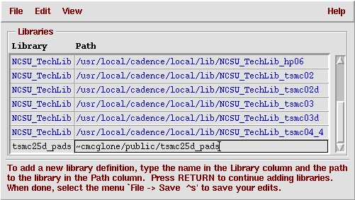
directory. In the Library Manager window, select
Edit->Library
          Path...
. Enter the name and path to the pad library in the window that appears as shown below. Then clickFile->Saveto activate the changes. You should then see thetsmc25d_padslibrary become available within the Library Manager window. (This is the easier option.)
Once you have the pad library available to you within your Cadence environment, you are ready to construct your pad frame. Refer to the
mini_framecell for a sample assembled pad frame. You will construct your pad frame by instantiating instances from the pad library into a new layout cell within your design library (from Virtuoso, clickCreate->Instance..., then clickBrowsein the window that appears, locate thetsmc25d_padslibrary and select the appropriate pad cells). The specific pad cells you require and the size of your pad frame will depend on the number and type of pins present in your design. Below is a brief description of the more common pad cells you will likely be using. The term core refers to the totality of your design that gets placed inside the pad frame (core + pad frame = die; die + package = chip).-
PadVdd- Vdd pad (supply to both pad frame and core) -
PadGnd- Gnd pad (supply to both pad frame and core) -
PadInC- buffered input pad with complement input (to core) -
PadOut- buffered output pad -
PadIO- unbuffered I/O pad with low ESD protection -
PadBiDirHE_025- buffered bi-directional pad with active-high enable -
PadNoConnect- pad cell with no connection to core -
PadlessSpacer- frame cell without pad connection -
PadlessCorner- corner frame cell
Be sure to adhere to a few rules when making your frame:
-
Your pad frame must create a complete ring (i.e. square or rectangle). In other words, each pad frame cell must be adjacent to another pad frame cell on either side -- no dangling ends. This is because the pad frame itself is a circuit that requires power and ground and each of the pad frame cells relies on its neighbor cells to provide those services. Use the
PadlessCornercell at each corner of your frame. -
At least one
PadVddandPadGndpad cell is required in the frame. This should not be a problem anyway since your core will require these signals, but even if somehow the core did not, the pad frame itself still requires these signals. -
Ensure that adjacent pad cells connect properly; the alignment is not arbitrary. Refer to the
mini_framesample for correct alignment/connection.
When your pad frame is complete, don't bother running DRC. The CMOS025/DEEP pad frame library takes advantage of the deep sub-micron scalable CMOS design rules (SCMOS_DEEP) which our Cadence installation does not currently support (or more precisely, the NCSU CDK does not, which is what we use). As such, the pad frame will fail DRC (it can also take several minutes to run).
With the pad frame finished, you are ready to insert your core and perform the necessary pad/core signal routing. First be sure to surround your core with power/ground rings for better and easier power distribution. Then route each of your top-level signals from your core to the appropriate point on the inner side of each of the pad cells. You can use Virtuoso'sConnectivity->Mark Netfeature to verify you have connectivity from each pad to the corresponding internal node of your core (click on the external pad node and ensure your core node becomes highlighted). Note that the Vdd and Gnd pad cells use Metal 1 for connection to the core whereas all other pad cells (for signals other than Vdd and Gnd) use Metal 2.Once the pad frame, core, and associated routing are complete, you're done. As mentioned before, the pad frame will not pass DRC. You can, however, if desired, run DRC on the pad frame by itself, note the total number of warnings/errors, then run DRC on the finished pad frame/core layout and ensure the same number of warnings/errors are detected. This will provide you with some confidence that your pad/core signal routing did not introduce any new DRC errors. Also, LVS is not an option because the schematic equivalents of the pad cells are not available. However, this does not prevent us from being able to extract the complete overall layout and running top-level simulations through the pad frame. If we include parasitics when we perform the extraction, the simulation results will give us the most realistic prediction of the behavior of our fabricated design.
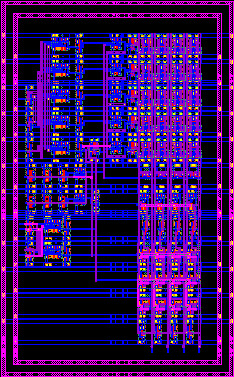
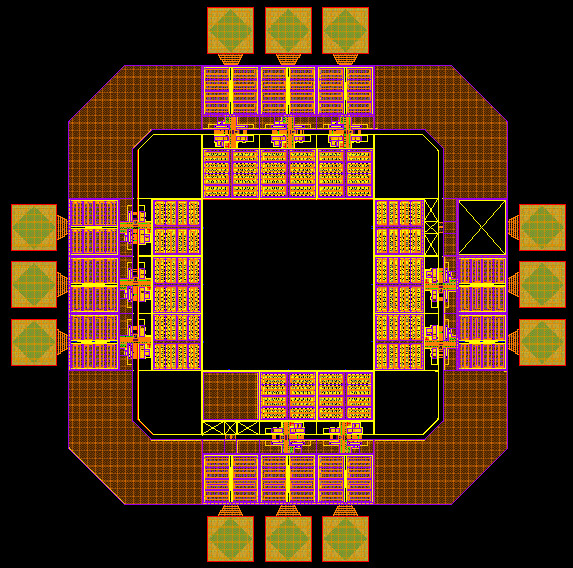
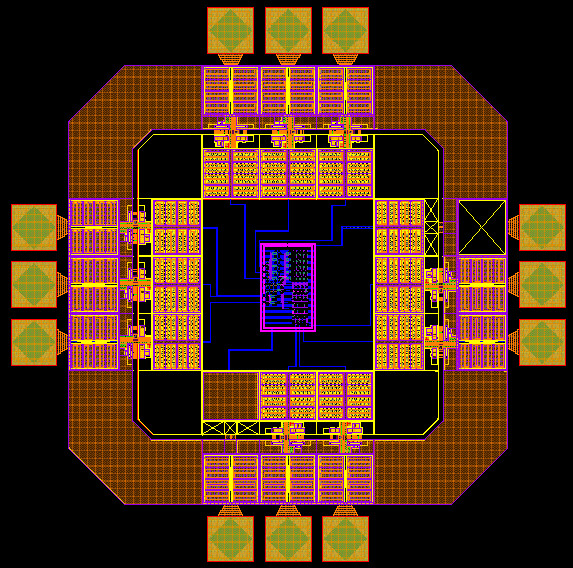
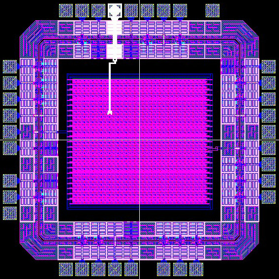
Following are some sample pictures illustrating the pad frame portion of the design process:
-
Sample Core with Power Ring - surround your core with larger than minimum width metal supply rings (Vdd and Gnd). Connect to each cell row of your core from both sides of the ring; use multiple contacts to ensure good connections.
-
Sample Pad Frame - construct the pad frame choosing the shape, size, and pad types required by your design.
-
Sample Pad Frame with Core - insert your core and perform the pad/core signal routing. Connect the Vdd/Gnd pads to the corresponding power ring rails. Be sure to use the correct metal layer to make contact with each pad cell.
-
Sample Pad Frame with Connectivity to Core - use Virtuoso's
Connectivity->Mark
          Net
feature to verify connectivity from the external pad to the target internal core node.
- Download the pad library from the MOSIS website
(I suggest GDS format) and use Cadence's import function (
- What
information should I include in my final project report?
Adhere to the guidelines presented in the Final Report Memo handed out in class (and available on Vista). Keep in mind that you are to submit a final project report, not a final project data sheet nor any other style of document. A project report is a technical document presenting the totality of your project, from initial concept through to results and conclusions, covering all relevant stages of design, analysis, and implementation in between. It is also a formal document, written in paragraph format (i.e. full-scale exposition as opposed to a simple concatenation of diagrams, equations, plots, figures, and output). You can assume that your audience for the report is technically inclined, but do not assume that they are experts in the field focused on by your project. Be sure to provide any necessary background, context, and/or references to other technical material needed to understand the functionality of your design.The length of the final project report can vary significantly based on the specifics and nature of the individual project, so pinpointing a particular target number is virtually impossible. The best piece of advice is to be thorough; touch on each and all items identified in the Final Report Memo, in addition to any other issues of relevance to your specific project. It is your job as a design team to present a convincing argument to your audience that you have at least considered all facets of your project. Even simply to address an issue and acknowledge that it can be safely disregarded for your design (and briefly explain why) is generally safer than to say nothing at all. Omitting discussion of a design aspect entirely risks the possibility that your audience/customer will perceive the omission as a gaping design hole.
With that said, when comparing reports of equal quality, shorter is always better. The less amount of space and detail it takes for you to capture a technically coherent presentation of your project, the more powerful your report will be. Keep in mind that it is generally easier to write a longer report -- not the other way around. Determining the minimal amount of information needed to lead your reader from point A (someone who is interested in learning more about your project) to point B (someone who now has a technical appreciation and understanding for the details of your design) by way of the most direct path requires extra time and effort to identify. For each figure/table/plot/printout in your design, try asking the following questions: what is the purpose of including this item? what is the value added by including this item? If you have any difficulty whatsoever answering either of those questions, it's probably better to yank the item.
Here is a review of the different subjects that should be included in the final report (straight from the memo):
- Abstract - brief synopsis; write this last.
- Introduction - a sizeable section addressing key high-level issues and background specific to your project; most important section in that it lays the groundwork for future sections.
- Project Description - the bulk of your report, including a system block diagram, component design, chip operation, floorplanning/layout, and any other key architectural features of your project. Include your top-level core layout and your final chip layout (including pad frame). You can include additional layouts for any key/interesting modules, but avoid including layouts for trivial cells and/or similar cells (e.g. fast vs. slow gate). For the final chip layout file, you can export your top-level layout (including the pad frame) using the instructions under the Quick-Start Guide, and include the path to the file in your report. DO NOT e-mail this file to the TA. The instructor will have an opportunity to review your layout during team interviews.
- Layout Verification - specific discussion regarding the LVS process and your results. You must include your top-level LVS output in your report. You do not need to include LVS output for any sub-cells (unless your top-level LVS fails, in which case you may want to include sub-cell LVS output for partial credit).
- Schematics/Simulations - transistor-level schematics for all key design modules, top-level system schematics used during chip validation and operation verification, and key simulation results used in design optimization and testing. Discuss testing strategy and approach. Omit trivial circuits and/or duplicate simulation results (i.e. it is okay simply to report and tabulate the results of multiple simulations after explaining and demonstrating the general process used to obtain them).
- Design Scaling - discuss the next-generation version of your chip and a brief overview of the development required to achieve it.
- Low-Power Features/Power Consumption - report power consumption results for your design as a function of chip mode, operation, and temperature (if relevant). Discuss any attractive low-power advantages your design offers.
- Testing - discuss the manufacturing testing of your chip (note that this does not refer to the design validation testing you perform with the simulator, but rather how to differentiate good chips from bad chips during the manufacturing process).
- Additional Information - discuss how your team negotiated the design of your project and delegated work amongst team members (and the rationale for doing so). Comment on responsibilities, accomplishments, and any obstacles or setbacks encountered and your method for handling them. If your final results did not meet your design goals, discuss possible causes and reasonable projections (in terms of time and effort) required to remedy them.
- Course Critique - although not anonymous in this case, honesty is always appreciated.
- Summary/Conclusions - tie your results back in with your introduction to evaluate the quality/effectiveness of your design. Recap what was accomplished and put it in perspective for your reader.
Feel free to reorder/restructure the subject list identified above in your own project report. Again, just be sure to touch on each of the areas requested.