Previous and current Research
Electronic pill for medication compliance monitoring: Electronic pill is design to help regulate the medication compliance, which costs drag developing companies billions of dollars per year. Up to date, the accurate measure of the medication compliance can only obtained by direct observation. The proposed e-pill is a device which can show itself from inside of the GI tract. Without affecting the capsule as a vessel for medication, the electronic device including the miniature radiating structure and the integrated electronics is attached to the outside of the standard sized capsule. Unique ID will be assigned to each device in future designs, which will help identify different medications and will provide a way to count the ingested pills.
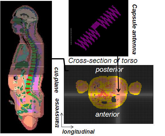
EM modeling: The study of small capsule antennas radiating from inside of human body is the foundation of the e-pill design. Many miniature antennas, such as loop antenna, straight line and zigzagged dipoles, were placed inside of a human body model, which is composed of 23 types of tissues with different electrical properties. Those antennas were tuned to various FCC regulated frequency bands by enforcing a reactance with the proper value across the antenna input, and the near- and far- field radiation characteristics of those antennas at each frequency band were simulated using finite difference time domain (FDTD) method.
Backscattering sensor: The frontier UHF radio frequency identification (RFID) tag designs utilize the idea of backscattering. A backscattering tag is completely passive, and the required DC supply is converted from the captured RF power by a voltage multiplier stage. When impinged with the tag antenna, the incoming RF power is scattered to all the directions in space. The backscattered power refers to the power that is reflected directly back to the RF transmitter. Different backscattered power levels are generated by different reflection coefficients at the antenna/chip interface. Based on this principle, to show its presence, the tag IC modulates (change the antenna loading) the tag antenna at a fixed rate to produce two alternative backscattered power levels, which generate distinguishable sidebands in frequency domain. includes a low power MHz range ring oscillator, a constant Gm sub-threshold bias generator circuit, a low drop-off voltage regulator, a RF demodulator for receiving command from the reader, a simple digital core to process the received command, and a register bank which stores the 8-bit unique ID of the tag. A three-stage RF multiplier is used to generate the DC supply voltage for all the integrated electronics.
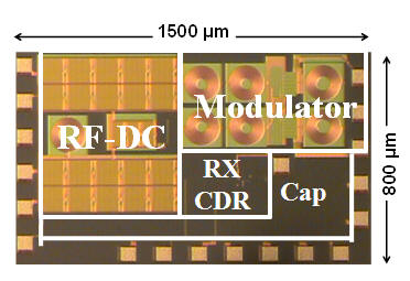
E-burst sensor: The IEEE regulation of human body exposure to RF power [9] limits the maximum power that can be used to power the passive tags. Under this regulation and considering the high attenuation for UHF signal passing through the human body, the backscattering tag can barely be turned on. However, the regulation allows human body exposure to higher power level at HF/VHF frequencies. Motivated by this fact, power conditioning is proposed. The passive tag can be activated by HF/VHF AC power transmitted through human body area network (BAN), and high power UHF bursts can be generated to show the pill presence from inside of the GI tract. Since the human body can be treated as a complex network composed of segment capacitors/resistors, power transfer channel is established by directly contacting the human body with conductive pads. No UHF burst (915MHz) is generated until the captured AC power reaches a pre-determined threshold value. To facilitate the e-burst function, command including the burst tuning word is modulated onto the power carrier by Amplitude Shift Keying/ Pulse Position Modulation (ASK/PPM), and a low power demodulator/ Clock-and-Data Recovery (CDR) circuit is implemented to download the command. High power UHF bursts (~0dBm) are generated by a 6-bit Digital Control Oscillator (DCO), and a class-D power amplifier. A carefully designed hysteresis comparator monitors the DC voltage on the storage capacitor, which controls the time duration of the UHF burst; All RF/analog blocks are biased by a constant Gm bias generator working in sub-threshold region; The digital controlling core including 20-bit First-In-Fist-Out (FIFO) register bank with 3-bit Cyclic Redundancy Check (CRC) is included to check the downloaded command. Similar to the aforementioned backscattering sensor, the required DC supply for the integrated electronics is converted from the HF/VHF AC power by a RF multiplier stage. The conversion efficiency of the multiplier is optimized by applying the charge equilibrium principle while assuming a constant load current and voltage.
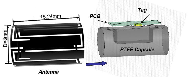
Miniature antenna design: Various miniature antennas were designed for the electronic pills. The antennas are first coarsely designed as a planar structure using ADS momentum. Then, the antennas are wrapped and simulated using FDTD method, and antenna traces tweaked until the input impedance reaches the target value. The designed miniature antennas were directly printed onto the curvature surface of the capsules by screen- or pad- printing method, and their performance were evaluated on a modified manual probe station using the network analyzer.
|
|
|
 |
|
Fig.1 EM modeling |
Fig.2 E-burst chip in CMOS130nm Technology |
Fig.3 Pill antenna and e-pill assembly |
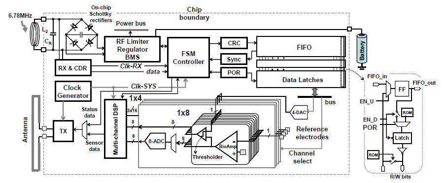
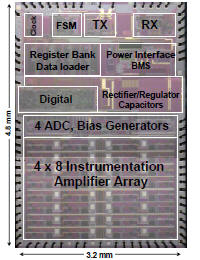
Multi-channel neural recording system: To help scientist study the neural activities inside the brain, the ambitious goal of our group is to design a low power implantable micro-system that composed all the necessary circuit blocks. The proposed design is capable of amplifying multiple neural signals simultaneously, converting the signal into digital bits, forming the converted bits into packages, and sending the packetsto a receiving unit wirelessly. The first version of the micro-system integrates 32 neural amplifiers, which is capable of recording 8 neural signals simultaneously. The amplified neural signals are converted into digital bits by 8-bit ADCs, and the data are formed into packet by an integrated processor. The data packet is sent out by an active UHF power oscillator. The micro-system is powered by a miniature re-chargeable battery, and a Battery Management System (BMS) is also implemented, which switches the system among different modes as operation, low battery, charging, etc. A wide dynamic range receiver chain including the RF front-end and ASK-PWM clock-and-data recovery circuit is integrated to download command from the base station. The first version of the micro-systems was fabricated using CMOS 0.5um and 130nm technology.
|
|
 |
|
Fig.4 Block Diagram of the neural recording micro-system |
Fig.5 Fabricated Chip in CMOS0.5um technology |
Antenna design for weather profiling radar: A two-frequency, dual-polarized antenna was designed for a weather profiling radar, which will perform polarimetric cloud measurements at 13.4 GHz, 35.6 GHz and 94.92 GHz. The dual band antenna is composed of a 13.4GHz corrugated horn antenna and a 35.6GHz dielectric rod waveguide located at the center of the horn antenna, and is able to generate parallel and vertical polarized radiation simultaneously at both bands. The fabricated antenna shows high polarization purity (less than -30dB cross-polarized product at both frequency bands).
Fig.6 The fabricated dual band, dual polarized antenna
Future Research Objectives
CMOS RF/analog low power electronics design: In the past 20 years, Moore’s Law correctly described the trend of the IC scaling, and it is predicted that this trend will continue for the next 10 years. To integrate more transistors on a limited area, the supply voltage will continue to drop in order to reduce the overall power consumption. While digital design can take the advantages of the process scaling by allowing the transistors operating under lower supply voltage, RF and analog circuit design becomes a more difficult and interesting task. In order to be complied with the reduced voltage headroom, while achieve better noise and linearity performance, many circuit functional blocks need to be re-studied, and new design techniques need to be developed, which requires the researcher to have fundamental understanding of the art of circuit design.
Micro-system integration for bio-medical related applications: The bio-medical related micro-system has the potential to revolutionize the medicare industry. Small and robust smart bio-sensors can monitor the biological signs, such as temperature, heartbeat, glucose level, etc., possibly at anywhere, anytime. Those devices are required not only to be capable of monitoring and recording, but to communicate with the external receiver/ computer system. The limited power and signal processing capability represent the current challenge in the design of the smart sensors. Sensors need to be implanted or digested introduce another major challenge: system minimization; the entire system including the miniature antenna and the integrated IC chip need to tightly fit into a package that is implantable or digestible. Furthermore, embedding the sensors within the biological environment add new requirements. For example, the system needs to be safe (bio-compatible), and ultra robust, which necessitate application specific solutions that are vastly different compared with traditional approaches. Design such a micro-system requires the solid understanding of EM theory, RF system and circuits, as well as sophiscated simulation and experimental skills.
