Project Description:
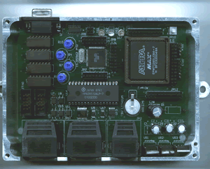
[left] Circuit Board with Billet Aluminum Enclosure [right] Enclosure Cover
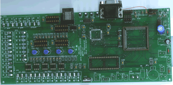
[top] Version 1
Project Background
Commissioned as part of the 2002-03 UF Formula SAE season, the SAE/DAQ was a chance to capture data from various vehicle mounted sensors. The original requirements were the ability to log at least 30 minutes of data from 18 sensors. Specifically, the sensors were 4 discrete wheel speed, 4 shock travel, 2 brake pressure, 4 discrete thermocouple, 2 axis accelerometer, rpm and steering wheel angle.
Processing Core
The heart of the system was the Atmel ATMega128 microcontroller (uC) and the Altera Max7128 Complex Programmable Logic Devic (CPLD).
The uC is an 8 bit RISC processor running at 11.592MHz. The ATMega128 included onboard peripherals such as a UART and an A/D converter. The uC primary duties include serial communication analog voltage to digital conversion, and memory management.
CPLD functions included 8 bit digital counters, memory strobe and chip selection, and upper address bit generation. The CPLD used 4 8 bit counters to count rising edge wheel sensor signals from the Hall type sensors. Another CPLD function was to aid in controlling of the external memory (512Kb). Further, the address latch (for the Atmel's multiplexed address and data bus) was located inside the CPLD. Lastly, the Altera piece generated the upper address lines for the additional memory, since the Atmel could only support 64Kb of external memory.
Sensors
The wheel speed sensors were Hall Effect sensors that generated a square pulse as ferrous material passed in front of it. Signal was passed through optoisolators to clean the rising edge and then further through inverting Schmitt triggers. The shock travel sensors amounted to a potentionmeter (a modified throttle position sensor) mounted to the bell crank. The four EGT sensors were Type K thermocouples rounted through Analog Devices AD595 thermocouple amplifiers. Circuitry was included to zero the sensors (see blue potentiometers above). The accelerometer is a 2 axis single chip solution from Analog Devices. RPM was directly recorded from a tachometer output. Last, steering wheel angle was again a potentiometer attached to the steering rack.
Memory
Memory was handled by a Hitachi 512Kx8 SRAM controlled with a Dallas NVRAM controller. The Dallas IC claimed 10 years of memory retention on a single 5V lithium cell.
Power
Board power was supplied through 3 discrete 5A power regulators. The 3 channels amounted to 5V, 8V, and 12V. The various voltage levels were required by the sensors. Raw input power was clamped at 14 volts by a Zener diode.
Serial Communication/UART
Serial communication is handled by the Atmel's on board universal asynchronous receiver/transmitter (UART). External circuitry included an RS232 line driver and charge pump capacitors.
ISP/JTAG Programming
The ATMega128 was programmed through Atmel's proprietary In-System Programming (ISP) protocol via an ISP header. The Altera CPLD is programmed through a standard JTAG port.
RE:Vision 2
RE:Vision 2's only major changes included 4 layer PCB design, new Hirose 8 and 12 position connectors, and surface mount resistors and capacitors. The overall footprint of the board was signifcanly reduced. Lastly, an aluminum enclosure was CNC'd out of a billet block of aluminum.