Project Description:
The ATMega 8535 Development board was designed, basically, because I could. I wanted another development environment in addition to my Atmel STK500 that included a CPLD.
RE:Vision 1
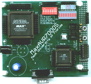
Version 1 included all of the essentials that I deemed necessary for a successful development environment. Features include fully socketable (and thus easily replaceable) master components, pulled up dip switches and led banks, full RS232 UART, external and internal clock sources including space for a 32.768kHz watch crystal. Also included is a small prototyping area. Connections between the CPLD and Atmel are made via wire jumpers, allowing increased development flexibility.
RE:Vision 2
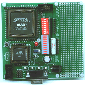
New features for Version 2 include smaller component area and increased prototyping area. Overall board size remains approximately the same. A clock source was added for the CPLD as well as JTAG programming. The last new feature is a header area ideally suited for servo connection.
Currently, no revision 3 is planned. The only possible changes could be a multilayer design with internal power and ground planes to further reduce size and increase noise immunity and the addition of a socketable crystal for the CPLD (vs. surface mount).